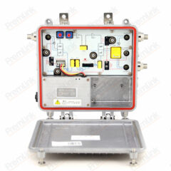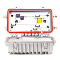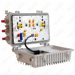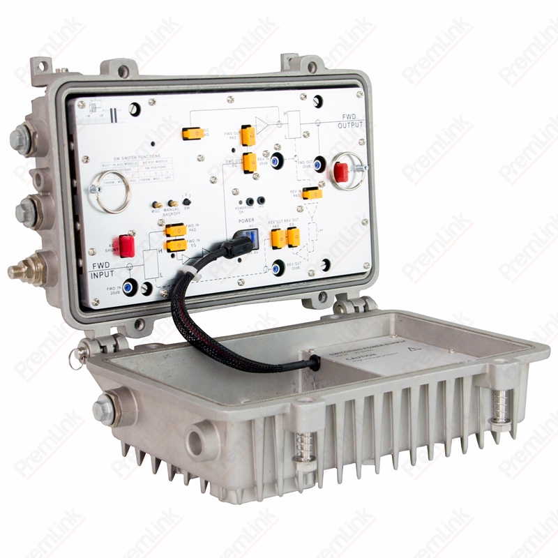
PL3600A broadband RF Amplifier is designed for fiber deeper HFC networks. PL3600A broadband RF Amplifier has two high level RF outputs that can be split to four lower level output ports. All attenuation and equalization changes will be set using standard JXP type pads. PL3600A broadband RF Amplifier will be field upgradable from a forward only to a forward and reverse path product.
Specifications
Forward Path Characteristics
| Parameter | Unit | Value | Remark |
| Frequency Range | MHz | 54 ~ 1002 | Different split is available |
| Gain | dB | 42 | 2 ports Version |
| Gain | dB | 38.5 | 4 ports Version |
| Internal Tilt | dB | 12±1 | @1002MHz |
| Flatness | dB | ±0.75 | -40℃ ~ +60℃ |
| Gain Thermal Stability | dB | ±1.5 | Under -40℃ ~ +60℃, output level is maintained and flatness is ±0.75dB over this temperature range. |
| Output Return Loss | dB | ≥16 | |
| RF Connector | / | 5/8” or PG11 | Exchangeable |
| RF Output TP | dB | -20±1 (w/jmpr) | Relative to RF output port, TP is F-female type connector |
| dB | -16.5±1(w/spltr) | ||
| Test Point Flatness | dB | ±0.75 | 2 ports Version |
| dB | ±1 | 4 ports Version | |
| Test Point Return Loss | dB | ≥16 | |
| Isolation | dB | 40 | In band, loop isolation |
| dB | 20 | Out of band, loop isolation | |
| dB | 15 | Crossover band, loop isolation | |
| Distortion Test Condition: RF output | dBmV | 50 | 2 ports version |
| dBmV | 46.5 | 4 ports version | |
| Distortion Test Condition: Tilt | dB | 12±1 | @1002MHz, cable tilt. |
| CTB | dBc | 67 | 79NTSC |
| CSO | dBc | 65 | 79NTSC |
| Cross Modulation | dBc | 62 | 79NTSC |
| Noise Figure | dB | <9 | |
| HUM | dB | 65 | @10A |
Return Path Characteristics
| Parameter | Unit | Value | Remark |
| Frequency Range | MHz | 5 ~ 42 | Different split is available |
| Gain | dB | 23 | Without 3-state switch |
| Flatness Reverse | dB | ±0.75 | |
| Internal Reverse Tilt | dB | 0 | ±0.5dB |
| Noise Figure | £ 10dB | Without 3-state switch, 2 ports output. | |
| Input Test Point | dB | -20 (w/jumper) | Relative to RF input port, ±1dB margin,
TP is F-female type connector |
| dB | -23.5 (w/splitter) | ||
| TP Flatness | dB | ±1.0 | |
| Reverse Return Loss | dB | ≥16 | |
| HUM | dB | 65 | @10A, Using the Matrix method |
General Characteristics
| Parameter | Unit | Value | Remark |
| Working Temperature | ℃ | -40 ~ +60 | |
| Storage Temperature | ℃ | -40 ~ +85 | |
| Output Ports | / | 2 or 4 | with splitter |
| Surge | kV | ±6 | IEEE C62.41, 1.2/50uS Combination Wave |
| Forward Equalizers | / | Plug-in(with JXP ATT) | |
| Return Equalizers | / | Plug-in(with JXP ATT) | Will be built based on different frequency split |
| Thermal Compensation | / | Yes | Built on board and only for Amplifier over TEMP compensation |
| AC Input Voltage | VAC | 40 to 90 | Line Powered |
| Efficiency | % | >80 | |
| Power Consumption | W | ≤35 | With Return path module |
| Power Passing | A | 10 or 15 exchangeable | 15A or 20A for 2 Hours@60°C no degradation is required for 10A or 15A respectively. |
| Water & Dust Resistance | / | IP68 | |
| Housing Dimensions | mm | 333*208*136 | Strand outdoor housing |
| Packaging Carton | mm | 370*270*220 | |
| Weight | 6Kg |
Welcome to enquiry our PL3600A Broadband RF Amplifier.