


Product Overview
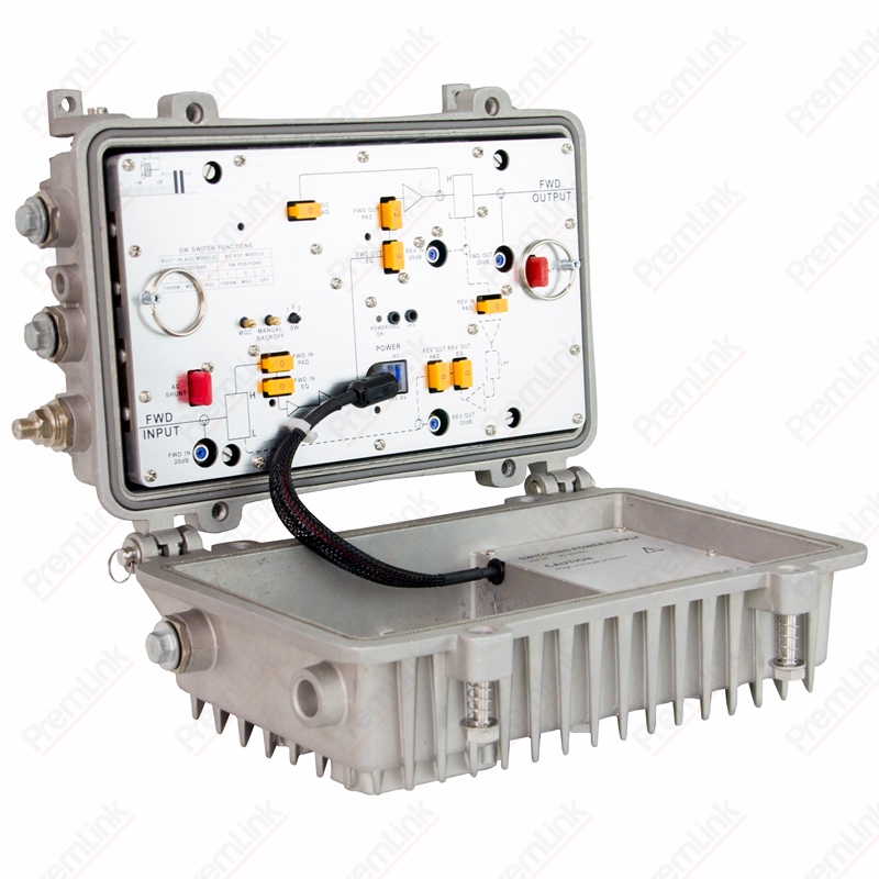
PL3600A broadband RF Amplifier is designed for fiber deeper HFC networks. PL3600A broadband RF Amplifier has two high level RF outputs that can be split to four lower level output ports. All attenuation and equalization changes will be set using standard JXP type pads. PL3600A broadband RF Amplifier will be field upgradable from a forward only to a forward and reverse path product.
Specifications
Forward Path Characteristics
| Parameter | Unit | Value | Remark |
| Frequency Range | MHz | 54 ~ 1002 | Different split is available |
| Gain | dB | 42 | 2 ports Version |
| Gain | dB | 38.5 | 4 ports Version |
| Internal Tilt | dB | 12±1 | @1002MHz |
| Flatness | dB | ±0.75 | -40℃ ~ +60℃ |
| Gain Thermal Stability | dB | ±1.5 | Under -40℃ ~ +60℃, output level is maintained and flatness is ±0.75dB over this temperature range. |
| Output Return Loss | dB | ≥16 | |
| RF Connector | / | 5/8” or PG11 | Exchangeable |
| RF Output TP | dB | -20±1 (w/jmpr) | Relative to RF output port, TP is F-female type connector |
| dB | -16.5±1(w/spltr) | ||
| Test Point Flatness | dB | ±0.75 | 2 ports Version |
| dB | ±1 | 4 ports Version | |
| Test Point Return Loss | dB | ≥16 | |
| Isolation | dB | 40 | In band, loop isolation |
| dB | 20 | Out of band, loop isolation | |
| dB | 15 | Crossover band, loop isolation | |
| Distortion Test Condition: RF output | dBmV | 50 | 2 ports version |
| dBmV | 46.5 | 4 ports version | |
| Distortion Test Condition: Tilt | dB | 12±1 | @1002MHz, cable tilt. |
| CTB | dBc | 67 | 79NTSC |
| CSO | dBc | 65 | 79NTSC |
| Cross Modulation | dBc | 62 | 79NTSC |
| Noise Figure | dB | <9 | |
| HUM | dB | 65 | @10A |
Return Path Characteristics
| Parameter | Unit | Value | Remark |
| Frequency Range | MHz | 5 ~ 42 | Different split is available |
| Gain | dB | 23 | Without 3-state switch |
| Flatness Reverse | dB | ±0.75 | |
| Internal Reverse Tilt | dB | 0 | ±0.5dB |
| Noise Figure | £ 10dB | Without 3-state switch, 2 ports output. | |
| Input Test Point | dB | -20 (w/jumper) | Relative to RF input port, ±1dB margin,
TP is F-female type connector |
| dB | -23.5 (w/splitter) | ||
| TP Flatness | dB | ±1.0 | |
| Reverse Return Loss | dB | ≥16 | |
| HUM | dB | 65 | @10A, Using the Matrix method |
General Characteristics
| Parameter | Unit | Value | Remark |
| Working Temperature | ℃ | -40 ~ +60 | |
| Storage Temperature | ℃ | -40 ~ +85 | |
| Output Ports | / | 2 or 4 | with splitter |
| Surge | kV | ±6 | IEEE C62.41, 1.2/50uS Combination Wave |
| Forward Equalizers | / | Plug-in(with JXP ATT) | |
| Return Equalizers | / | Plug-in(with JXP ATT) | Will be built based on different frequency split |
| Thermal Compensation | / | Yes | Built on board and only for Amplifier over TEMP compensation |
| AC Input Voltage | VAC | 40 to 90 | Line Powered |
| Efficiency | % | >80 | |
| Power Consumption | W | ≤35 | With Return path module |
| Power Passing | A | 10 or 15 exchangeable | 15A or 20A for 2 Hours@60°C no degradation is required for 10A or 15A respectively. |
| Water & Dust Resistance | / | IP68 | |
| Housing Dimensions | mm | 333*208*136 | Strand outdoor housing |
| Packaging Carton | mm | 370*270*220 | |
| Weight | 6Kg |
Welcome to enquiry our PL3600A Broadband RF Amplifier.
PL3600A: 1.2GHz High-Performance GaN Broadband RF Amplifier
Designed for DOCSIS 3.1 architectures, the PL3600A combines GaN efficiency with 1.2GHz bandwidth to deliver massive data capacity over deep-fiber HFC networks.
- DOCSIS 3.1 Ready (1.2GHz): The PL3600A broadband RF amplifier expands your network capacity with support for up to 1200MHz bandwidth, ensuring full compatibility with multi-gigabit data services and expanded digital channel lineups.
- GaN + GaAs Hybrid Technology: By utilizing Gallium Nitride (GaN) power doubling technology, this amplifier achieves higher output levels and superior thermal efficiency compared to traditional GaAs-only designs, significantly reducing overall network power consumption.
- Triple Control Modes (AGC/MGC/Thermal): Offers ultimate operational flexibility with selectable Automatic Gain Control (AGC), Manual Gain Control (MGC), or Thermal Compensation modes to maintain rock-solid signal stability across volatile outdoor temperature swings.
- Modular Forward & Reverse Paths: Features a field-upgradable architecture. Start with a forward-only configuration and easily add a high-gain reverse path module (5-42/65/85/204MHz splits available) as your upstream bandwidth demand grows.
- Enhanced Surge & ESD Protection: Engineered with improved ±6kV surge protection and a precision thermal circuit for over-temperature compensation, guaranteeing long-term hardware reliability in the harshest outdoor environments.
Technical FAQ: PL3600A Broadband RF Amplifier
Q1: Why is GaN technology superior for 1.2GHz HFC networks?
A: As frequencies push toward 1.2GHz, signal loss increases. GaN (Gallium Nitride) allows the PL3600A broadband RF amplifier to provide higher gain and higher output levels with better linearity and lower noise than GaAs, which is critical for maintaining high MER/BER in DOCSIS 3.1 systems.
Q2: Can the PL3600A be configured for 4-port output?
A: Yes. The PL3600A features a flexible internal splitting architecture. It can be configured as a high-power 2-port amplifier (42dB gain) or, by using internal splitters, as a 4-port distribution amplifier (38.5dB gain) to suit different neighborhood distribution densities.
Q3: How does the plug-in JXP pad system simplify maintenance?
A: Like all Premlink professional-grade equipment, the PL3600A broadband RF amplifier uses standardized JXP-style plug-in pads for all attenuation and equalization settings. This eliminates the need for expensive proprietary components and allows technicians to balance the entire HFC plant with a single set of universal spare parts.
Upgrading to DOCSIS 3.1?
If your network roadmap requires extended spectrum above 1.2GHz or specific high-split return paths, pair this amplifier with our
PL3100A Series
for a comprehensive HFC coverage solution.


